


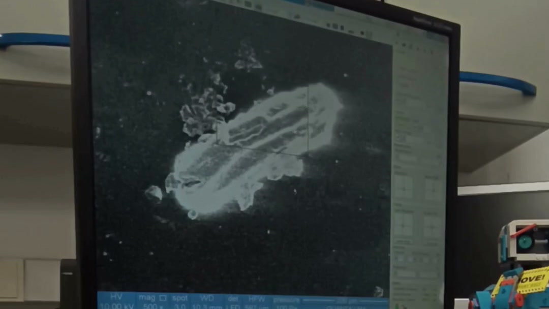
What actually happens during a scanning electron microscopy (SEM) session? This video offers a glimpse into one of the analytical techniques that supports our work at INMA (the Institute of Nanoscience and Materials of Aragón) within the IMASUS project.
Although a SEM image may look like a striking black-and-white photograph, every image begins much earlier. Samples must be carefully prepared, mounted, and introduced into the microscope’s vacuum chamber. Once inside, an electron beam scans the surface point by point, generating signals that are transformed into highly detailed images.
Unlike conventional optical microscopy, SEM allows us to observe the microstructure and surface morphology of materials at magnifications ranging from hundreds to tens of thousands of times, revealing features that would otherwise remain invisible.
Within IMASUS, SEM has become an essential tool for understanding sustainable fashion materials. For us at INMA, each microscopy session is an opportunity to look beyond what can be seen with the naked eye. Many of the properties that determine how a material behaves are hidden at the microscale, waiting to be explored.
We hope this short video brings you a little closer to the laboratory and shows how scientific research contributes to the broader goals of IMASUS. Sometimes, understanding a material starts by simply looking at it from a different perspective—and SEM allows us to do exactly that.
Enjoy the session!